SEMICONDUCTOR YIELD IMPROVEMENT KIT

The knowledge of Sea Synergy engineering does not stop at the depths of the ocean floor. This semiconductor yield improvement kit has EVERYTHING IN ONE place for yield engineers out there to find and/or collect defect samples from various locations in semiconductor processing equipment.

Tool_Kit.jpg

Below is the list of each tool and its use

Magnifier_open.jpg Mag_closed.jpg

Illuminated Magnifier: Use for detecting the smaller than 1x visible defects and compare surface roughness and/or textures such as grit blasted and arc spray.

Sissors.jpg

Ceramic Scissors: Eliminating all corrosion and cross contamination between samples being cut with iron or other metal materials.

Comparitor.jpg

Optical Comparator: It is a 6x optical comparator with measurement scale that allows a direct measurement of the defect size.

Ti_tweezers.jpg

Ti Tweezers: Use Ti tweezers for collecting all metals samples other than Ti.

Ceramic_tweezer.jpg
Grabber.jpg
UV_Light_365nm.jpg
UV_Light_400nm.jpg
White_light.jpg
Laser_pointer.jpg
Space_pen.jpg
Sharpie.jpg

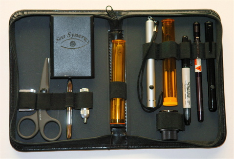
Ceramic Tweezers: Use ceramic tweezers for collecting all metals samples.

Sample Holder: Equipped with 3 metal fingers to grip/hold sample strips/stub to collect samples in tight/small areas

365nm UV Light

400nm UV Light

UV Lights: The different UV wavelength lights help to identify different organic contamination.

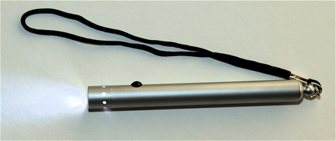
White LED Light: This high intensity light helps to identify defects in areas with yellow lights.

Red Laser Pointer: Identify the exact sample location.

Black Ink Pen: Write well on most cleanroom paper.

Permanent Marker: Mark defect sample holders such as plastic bag/bottle.

[Home] [Products] [Wipers] [Shark] [Stargate] [Yield Kit] [LMH Kit] [Remora] [Order]